- 您现在的位置:买卖IC网 > Sheet目录3880 > PIC18F23K20-I/MV (Microchip Technology)IC MCU 8BIT 8KB FLASH 28UQFN
dsPIC33F
DS70165E-page 178
Preliminary
2007 Microchip Technology Inc.
15.1.4
DOUBLE UPDATE MODE
In the Double Update mode (PTMOD<1:0> = 11), an
interrupt event is generated each time the PTMR regis-
ter is equal to zero, as well as each time a period match
occurs. The postscaler selection bits have no effect in
this mode of the timer.
The Double Update mode provides two additional
functions to the user. First, the control loop bandwidth is
doubled because the PWM duty cycles can be updated,
twice per period. Second, asymmetrical center-aligned
PWM waveforms can be generated, which are useful for
minimizing output waveform distortion in certain motor
control applications.
15.1.5
PWM TIME BASE PRESCALER
The input clock to PTMR (FOSC/4) has prescaler
options of 1:1, 1:4, 1:16 or 1:64, selected by control
bits, PTCKPS<1:0>, in the PTCON SFR. The prescaler
counter is cleared when any of the following occurs:
a write to the PTMR register
a write to the PTCON register
any device Reset
The PTMR register is not cleared when PTCON is
written.
15.1.6
PWM TIME BASE POSTSCALER
The match output of PTMR can optionally be post-
scaled through a 4-bit postscaler (which gives a 1:1 to
1:16 scaling).
The postscaler counter is cleared when any of the
following occurs:
a write to the PTMR register
a write to the PTCON register
any device Reset
The PTMR register is not cleared when PTCON is written.
15.2
PWM Period
PTPER is a 15-bit register and is used to set the counting
period for the PWM time base. PTPER is a double-
buffered register. The PTPER buffer contents are loaded
into the PTPER register at the following instants:
Free-Running and Single-Shot modes: When the
PTMR register is reset to zero after a match with
the PTPER register.
Up/Down Count modes: When the PTMR register
is zero.
The value held in the PTPER buffer is automatically
loaded into the PTPER register when the PWM time
base is disabled (PTEN = 0).
The
PWM
period
can
be
determined
using
EQUATION 15-1:
PWM PERIOD
If the PWM time base is configured for one of the Up/
Down Count modes, the PWM period will be twice the
value provided by Equation 15-1.
The maximum resolution (in bits) for a given device
oscillator and PWM frequency can be determined using
EQUATION 15-2:
PWM RESOLUTION
15.3
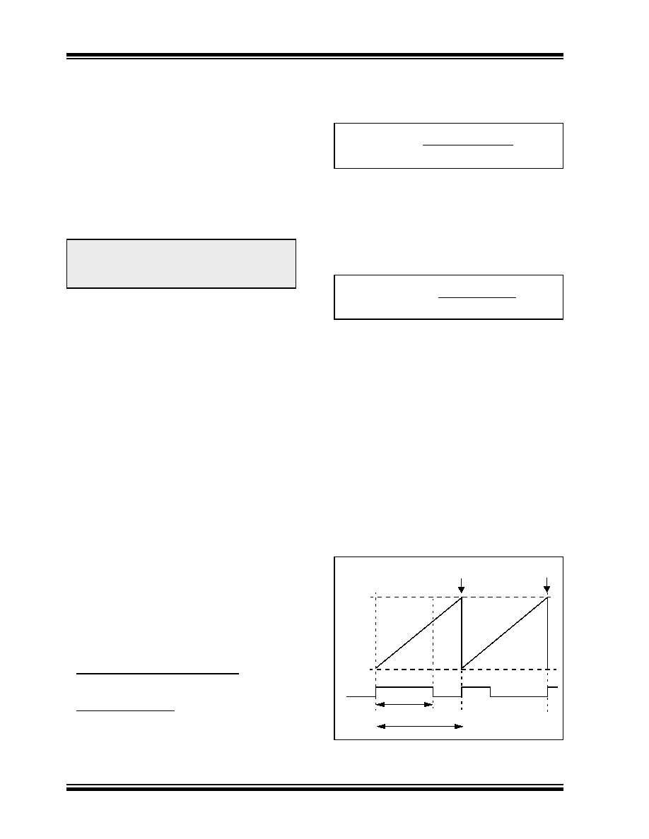
Edge-Aligned PWM
Edge-aligned PWM signals are produced by the module
when the PWM time base is in Free-Running or Single-
Shot mode. For edge-aligned PWM outputs, the output
has a period specified by the value in PTPER and a duty
cycle specified by the appropriate Duty Cycle register
(see Figure 15-2). The PWM output is driven active at
the beginning of the period (PTMR = 0) and is driven
inactive when the value in the Duty Cycle register
matches PTMR.
If the value in a particular Duty Cycle register is zero,
then the output on the corresponding PWM pin will be
inactive for the entire PWM period. In addition, the out-
put on the PWM pin will be active for the entire PWM
period if the value in the Duty Cycle register is greater
than the value held in the PTPER register.
FIGURE 15-2:
EDGE-ALIGNED PWM
Note:
Programming a value of 0x0001 in the
PWM Period register could generate a
continuous interrupt pulse and hence,
must be avoided.
TPWM =
TCY (PTPER + 1)
(PTMR Prescale Value)
Resolution =
log (2 TPWM/TCY)
log (2)
Period
Duty Cycle
0
PTPER
PTMR
Value
New Duty Cycle Latched
发布紧急采购,3分钟左右您将得到回复。
相关PDF资料
PIC16F627A-I/P
IC MCU FLASH 1KX14 EEPROM 18DIP
XF2G-1414-11
CONN FPC 14POS 0.5MM SMT
PIC16F777T-I/ML
IC PIC MCU FLASH 8KX14 44QFN
PIC18F2539T-E/SO
IC PIC MCU FLASH 12KX16 28SOIC
PIC16LF1936-I/SO
IC PIC MCU FLASH 512KX14 28-SOIC
PIC16F873AT-E/ML
IC PIC MCU FLASH 4KX14 28QFN
PIC18F2439T-E/SO
IC PIC MCU FLASH 6KX16 28SOIC
PIC16LF777T-I/ML
IC PIC MCU FLASH 8KX14 44QFN
相关代理商/技术参数
PIC18F23K20-I/SO
功能描述:8位微控制器 -MCU 8 KB Enh Flash 768 RAM 25 I/O Pb Free RoHS:否 制造商:Silicon Labs 核心:8051 处理器系列:C8051F39x 数据总线宽度:8 bit 最大时钟频率:50 MHz 程序存储器大小:16 KB 数据 RAM 大小:1 KB 片上 ADC:Yes 工作电源电压:1.8 V to 3.6 V 工作温度范围:- 40 C to + 105 C 封装 / 箱体:QFN-20 安装风格:SMD/SMT
PIC18F23K20-I/SP
功能描述:8位微控制器 -MCU 8 KB Enh Flash 768 RAM 25 I/O Pb Free RoHS:否 制造商:Silicon Labs 核心:8051 处理器系列:C8051F39x 数据总线宽度:8 bit 最大时钟频率:50 MHz 程序存储器大小:16 KB 数据 RAM 大小:1 KB 片上 ADC:Yes 工作电源电压:1.8 V to 3.6 V 工作温度范围:- 40 C to + 105 C 封装 / 箱体:QFN-20 安装风格:SMD/SMT
PIC18F23K20-I/SS
功能描述:8位微控制器 -MCU 8 KB Enh Flash 768 RAM 25 I/O Pb Free RoHS:否 制造商:Silicon Labs 核心:8051 处理器系列:C8051F39x 数据总线宽度:8 bit 最大时钟频率:50 MHz 程序存储器大小:16 KB 数据 RAM 大小:1 KB 片上 ADC:Yes 工作电源电压:1.8 V to 3.6 V 工作温度范围:- 40 C to + 105 C 封装 / 箱体:QFN-20 安装风格:SMD/SMT
PIC18F23K20T-I/ML
功能描述:8位微控制器 -MCU 8 KB Enh Flash 768 RAM 25 I/O Pb Free RoHS:否 制造商:Silicon Labs 核心:8051 处理器系列:C8051F39x 数据总线宽度:8 bit 最大时钟频率:50 MHz 程序存储器大小:16 KB 数据 RAM 大小:1 KB 片上 ADC:Yes 工作电源电压:1.8 V to 3.6 V 工作温度范围:- 40 C to + 105 C 封装 / 箱体:QFN-20 安装风格:SMD/SMT
PIC18F23K20T-I/MV
功能描述:8位微控制器 -MCU 8KB Flash 768B RAM Enhanced Flash RoHS:否 制造商:Silicon Labs 核心:8051 处理器系列:C8051F39x 数据总线宽度:8 bit 最大时钟频率:50 MHz 程序存储器大小:16 KB 数据 RAM 大小:1 KB 片上 ADC:Yes 工作电源电压:1.8 V to 3.6 V 工作温度范围:- 40 C to + 105 C 封装 / 箱体:QFN-20 安装风格:SMD/SMT
PIC18F23K20T-I/SO
功能描述:8位微控制器 -MCU 8 KB Enh Flash 768 RAM 25 I/O Pb Free RoHS:否 制造商:Silicon Labs 核心:8051 处理器系列:C8051F39x 数据总线宽度:8 bit 最大时钟频率:50 MHz 程序存储器大小:16 KB 数据 RAM 大小:1 KB 片上 ADC:Yes 工作电源电压:1.8 V to 3.6 V 工作温度范围:- 40 C to + 105 C 封装 / 箱体:QFN-20 安装风格:SMD/SMT
PIC18F23K20T-I/SS
功能描述:8位微控制器 -MCU 8 KB Enh Flash 768 RAM 25 I/O Pb Free RoHS:否 制造商:Silicon Labs 核心:8051 处理器系列:C8051F39x 数据总线宽度:8 bit 最大时钟频率:50 MHz 程序存储器大小:16 KB 数据 RAM 大小:1 KB 片上 ADC:Yes 工作电源电压:1.8 V to 3.6 V 工作温度范围:- 40 C to + 105 C 封装 / 箱体:QFN-20 安装风格:SMD/SMT
PIC18F23K22-E/ML
功能描述:8位微控制器 -MCU 8KB Flash 768b RAM SERIAL EE IND RoHS:否 制造商:Silicon Labs 核心:8051 处理器系列:C8051F39x 数据总线宽度:8 bit 最大时钟频率:50 MHz 程序存储器大小:16 KB 数据 RAM 大小:1 KB 片上 ADC:Yes 工作电源电压:1.8 V to 3.6 V 工作温度范围:- 40 C to + 105 C 封装 / 箱体:QFN-20 安装风格:SMD/SMT